Отправить сообщение

Printed Circuit Board Laser Depaneling Machine For Stress Free Cutting

1 набор
MOQ
Negotiable
цена
Printed Circuit Board Laser Depaneling Machine For Stress Free Cutting
Характеристики Галерея Характер продукции Спросите цитату
Характеристики
Характеристики
Сила (в):: 10/12/15/18W
Располагать точность: μm ± 25 (1 Mil)
Доставка: ОБМАНЫВАЙТЕ/EXW/DHL
Размер: 1000mm*940mm *1520 mm
Охлаждать: С воздушным охлаждением (внутренний охлаждать вод-воздуха)
ИМЯ: Лазер depaneling
Высокий свет:

desiccant dry cabinets

,

dry storage cabinets

Основная информация
Место происхождения: КИТАЙ
Фирменное наименование: chuangwei
Сертификация: CE ROHS
Номер модели: КВВК-5Л
Оплата и доставка Условия
Упаковывая детали: каждый набор был упакован в случае переклейки
Время доставки: 7 дней работы
Условия оплаты: T/T, западное соединение, L/C
Поставка способности: 260 наборов в месяц
Характер продукции


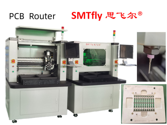
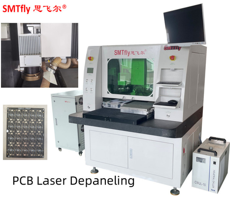
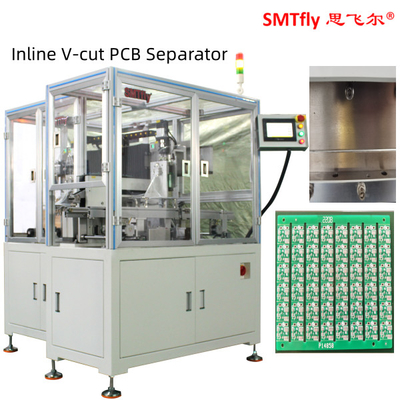
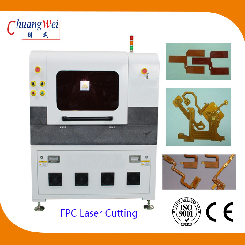
Laser Depaneling of Printed Circuit Boards (PCBs) for Stress-free Cutting


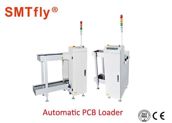
This systems can process even highly complicated tasks with printed circuit boards (PCBs). They are available in variants for cutting assembled PCBs, flexible PCBs and cover layers.


Process advantages

Compared to conventional tools, laser processing offers a compelling series of advantages.


  • The laser process is completely software-controlled. Varying materials or cutting contours are easily taken into account through adapting the processing parameters and laser paths.
  • In the case of laser cutting with the UV laser, no appreciable mechanical or thermal stresses occur.
  • The laser beam merely requires a few µm as a cutting channel. More components can thus be placed on a panel.
  • The system software differentiates between operation in production and setting up processes. That clearly reduces instances of faulty operation.
  • The fiducial recognition by the integrated vision system is done in the latest version around 100% faster than before.


Processing Flat Substrates

UV laser cutting systems display their advantages at various positions in the production chain. With complex electronic components, the processing of flat materials is sometimes required.
In that case, the UV laser reduces the lead time and total costs with every new product layout. It is optimized for these work steps.
 

  • Complex contours
  • No substrate brackets or cutting tools
  • More panels on the base material
  • Perforations and decaps


Integration in MES Solutions

The model seamlessly integrates into existing manufacturing execution systems (MESs). The laser system delivers operative parameters, machine data, tracking & tracing values and information about individual production runs.


Laser class 1
Max. working area (X x Y x Z) 300 mm x 300 mm x 11 mm
 
Max. recognition area (X x Y) 300 mm x 300 mm
Max. material size (X x Y) 350 mm x 350 mm
Data input formats Gerber, X-Gerber, DXF, HPGL,
Max. structuring speed Depends on application
Positioning accuracy ± 25 μm (1 Mil)
Diameter of focused laser beam 20 μm (0.8 Mil)
Laser wavelength 355 nm
System dimensions (W x H x D) 1000mm*940mm
*1520 mm
Weight ~ 450 kg (990 lbs)
Operating conditions  
Power supply 230 VAC, 50-60 Hz, 3 kVA
Cooling Air-cooled (internal water-air cooling)
Ambient temperature 22 °C ± 2 °C @ ± 25 μm / 22 °C ± 6 °C @ ± 50 μm
(71.6 °F ± 3.6 °F @ 1 Mil / 71.6 °F ± 10.8 °F @ 2 Mil)
Humidity < 60 % (non-condensing)
Required accessoires Exhaust unit
Порекомендованные продукты
Свяжись с нами
Контактное лицо : Eric Cao
Телефон : 86-13922521978
Факс : 86-769-82784046
Осталось символов(20/3000)